Designing a printed circuit board (PCB) on a computer can make everything look simple. Components snap neatly into place, spacing looks clean, and routing feels efficient. But what works on-screen doesn’t always translate well to real-world manufacturing.
At Southrock Engineering, we design and assemble custom PCBAs, as well as custom cables and wire assemblies, box builds, and reverse engineer printed circuit boards. We often see PCB designs that are electrically sound but unnecessarily expensive or difficult to assemble. The good news is that most of these issues can be avoided early in the design phase.
Keep reading to learn more about PCB Design for Manufacturing (DFM) and how to make your design more cost-effective, scalable, and production friendly.
New to electronics manufacturing? No problem! We’ve created glossaries for Basic PCB and PCBA Terms, Electrical Component Related Terms, PCB Soldering & Assembly Terms, and Manufacturing & Quality Control Terms. Have more questions? Check out our FAQs.
Why DFM Matters
The biggest misconception our engineers see that, “Parts are the main cost.” In reality, assembly is often the most expensive part of your project, especially for low-to-mid volume production.
Small design decisions can mean:
- More assembly steps
- Specialized equipment
- Slower production
- Higher failure rates
- Increased inspection time
DFM is about simplifying all of that.
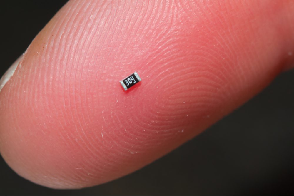
Component Size Matters More Than You Think

One of the most common (and costly) issues is using components that are too small.
For example: 0201 components (extremely small) vs. 0603 components (industry-standard and easier to handle)
While 0201 parts may look fine in CAD, they present real challenges:
- Difficult (or impossible) to assemble by hand for prototypes
- Require specialized high-volume production setups
- Harder to inspect and repair
- Significantly increase assembly cost
Best Practice:
Use 0603 components or larger whenever possible. In some cases, 0402 may be acceptable, but anything smaller should be carefully justified.
Design for Panelization (Build Multiple Boards at Once)
If your product uses multiple PCBs, don’t design them as completely separate units.
Instead, think about panelization:
- Combine multiple boards into a single manufacturing panel (or “pallet”)
- Allow all boards to be processed together in one pass
This reduces:
- Setup time
- Handling
- Assembly cost per unit
Example:
Instead of assembling three separate boards individually, they can be printed and soldered in one operation when grouped together.
Keep Assembly Simple (Fewer Steps = Lower Cost)
Every additional manufacturing step adds time and cost.
Some common cost drivers:
- Components on both sides of the PCB (requires multiple reflow cycles)
- Multiple separate boards instead of one combined board
- Complex shapes that require routing instead of simple scoring
- Through-hole components that require manual assembly
Best Practices:
- Place components on one side only whenever possible
- Use surface mount components (SMD) as much as possible, rather than through-hole components
- Combine boards if space allows
- Use rectangular board shapes for easier panelization and separation
- Minimize the number of PCB layers if your design allows
Surface mount components can be placed and soldered automatically, making production faster and more cost-effective.
Through-hole components, on the other hand, are typically installed and soldered by hand, which increases labor time and cost, especially as production scales. Use them only when necessary (for strength, connectors, or specific part requirements).
Avoid Vias in Pads (and Other Layout Pitfalls)
Certain layout choices can create major assembly problems, even if the circuit works electrically.
Common issues:
- Vias inside component pads
- Solder can flow into the hole during reflow
- Leads to weak or failed connections
- Vias hidden under components
- Makes inspection and troubleshooting difficult
- Components placed too tightly together
- Harder to assemble
- Harder to inspect
- Increases risk of defects
Best Practice:
- Keep vias outside of pads, connected with short traces
- Space components enough for inspection and rework
- Keep silkscreen labels clear and readable
Plan for Programming and Testing Early
If your board includes a microcontroller, it will need to be programmed. A common oversight is not designing a practical way to do this.
What works well:
- A simple row of accessible programming pins
- Standard spacing (e.g., 0.1″ pitch)
- Plated through-holes that allow temporary connections (no permanent connector required)
Instead of adding a dedicated connector to the PCB, you can use plated through-holes that match your programming pins. During production, a technician can temporarily insert or hold a programming header in place just long enough to load the firmware.
This Approach:
- Reduces component cost
- Saves space on the board
- Speeds up the programming process
For development or repeated use, a permanent connector may still make sense but for production, simpler is often better.
Think About Mechanical Assembly (Not Just Electronics)
Electrical design is only part of the picture. Mechanical fit matters too. If you’re trying to maintain a specific gap (e.g., 5 mm between boards):
- Consider using fixed-height standoffs or spacers instead of relying only on headers
- Use connectors with mechanical stops or pair headers with spacers for consistency
- Validate real-world tolerances—not just CAD dimensions
For Example:
- Stacked PCBs need consistent spacing
- Board-to-board connectors must physically fit and align
- Pin lengths and tolerances affect final assembly
Prototype Smart. Then Scale.
What works for a prototype doesn’t always scale efficiently. DFM means designing with production in mind from the start, even if you’re only building a few prototypes initially.
For Example:
- A design that requires delicate manual assembly may be fine for 3 units
- But becomes expensive or impractical at 100+ units
The Bottom Line
You can build almost anything but not everything is cost-effective to build. The earlier you consider manufacturing constraints, the more you can:
- Reduce costs
- Improve reliability
- Speed up production
- Avoid redesigns
The simpler your design is to manufacture, the more affordable and scalable it becomes.
Need a Second Set of Eyes on Your PCB Design?
At Southrock Engineering, we regularly review PCB designs before production to catch cost drivers early and suggest improvements.
If you already have Gerber files and a BOM, we can help you:
- Identify manufacturing risks
- Recommend cost-saving adjustments
- Prepare your design for efficient assembly

Blog Contributions by:
Peter Hall, President at Southrock Engineering